


Page 33 - january_123021.indd
P. 33
JANUARY 2022      TAP TIMES          -33-          In May 2021, the researchers announced a
                                                                2-nanometer node chip designs which will
                  IBM, Samsung (from 32)                        allow a chip to fit up to 50 billion transis-

                                                                tors in a space the size of a fingernail. VT-
        (FETs), such as fin field effect transistors,           FET continues the innovation journey, and
        or finFETs (which got its name because its              opens the door to new possibilities.
        silicon body resembles the back fin of a
        fish), which layers transistors along a wa-             Contacted Gate Pitch
        fer’s surface.                                          In the past, designers packed more tran-
                                                                sistors onto a chip by shrinking its gate
        Transistors in layers                                   pitch and wiring pitch. The physical space
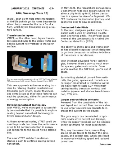
        VTFET, on the other hand, layers transis-               where all the components fit is called the
        tors perpendicular to the silicon wafer and             Contacted Gate Pitch (CGP).
        directs current flow vertical to the wafer
        surface.                                                The ability to shrink gate and wiring pitch-
                                                                es has allowed integrated-circuit designers
                                                                to go from thousands to millions to billions
                                                                of transistors in our devices.

                                                                With the most advanced finFET technolo-
                                                                gies, however, there’s only so much room
                                                                for spacers, gates and contacts. Once
                                                                you’ve reached the CGP limit, you’re out of
                                                                space.

                                                                By orienting electrical current flow verti-
        This is a side-by-side comparison of a a VFET (left) and a lateral   cally, the gates, spaces and contacts are
        FET are arranged with current flowing through them. (IBM)
                                                                no longer constrained in traditional ways:
        This new approach addresses scaling bar-                We have room to scale CGP while main-
        riers by relaxing physical constraints on               taining healthy transistor, contact, and
        transistor gate length, spacer thickness,               isolation (spacer and shallow trench isola-
        and contact size so that these features can             tion, STI) size.
        each be optimized; either for performance
        or energy consumption.                                  Larger source/drain contacts
                                                                Released from the constraints of the lat-
        Beyond nanosheet technology                             eral layout and current flow, we were able
        With VTFET, we’ve managed to successful-                to use larger source/drain contacts to in-
        ly demonstrate that it’s possible to explore            crease the current on the device.
        scaling beyond nanosheet technology in
        CMOS semiconductor design.                              The gate length can be selected to opti-
                                                                mize device drive current and leakage,
        At these advanced nodes, VTFET could be                 while the spacer thickness can be indepen-
        used to provide two times the performance               dently optimized for lower capacitance.
        or up to 85 percent reduction in energy
        use compared to the scaled finFET alterna-              This, say the researchers, means they
        tive.                                                   are no longer forced to tradeoff the gate,
                                                                spacer, and contact size, which can result
        The new VTFET architecture demon-                       in improved switching speed and reduced
        strates a path to continue scaling beyond               power use.
        nanosheet.                                                                                              ibm.com

