


Page 31 - january_123021.indd
P. 31
TAP TIMES      -31-                                   JANUARY 2022


           Intel shows and tells key tech                       This, says Intel, will provide an order of
                advances at IEDM meet                           magnitude increase in the interconnect
                                                                density for 3D stacking.

        SAN FRANCISCO — At the December                         New industry standards
        International Electron Devices Meet-                    To enable the ecosystem to gain benefits
        ing, Intel unwrapped what it termed                     of advanced packaging, Intel is also call-
        breakthroughs in chip packaging,                        ing for the establishment of new industry
        transistors and quantum physics.                        standards and testing procedures to en-
                                                                able a hybrid bonding chiplet ecosystem.
        10X density improvement
        These advances, according to Intel, are on              Looking beyond its gate-all-around Rib-
        the path to a 10X interconnect density im-              bonFET, Intel is mastering the coming
        provement in packaging with hybrid bond-                post-FinFET era with an approach to stack-
        ing; 30-50% area improvement in transis-                ing multiple (CMOS) transistors that aims
        tor scaling; and new concepts in physics.               to achieve a maximized 30% to 50% logic

                                                                scaling improvement for the continued ad-
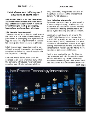
        Intel, the company says, is pursuing sig-               vancement of Moore’s Law by fitting more
        nificant research in essential scaling tech-            transistors per square millimeter.
        nologies for delivering more transistors in
        future product offerings:                               Intel is also paving the way for Moore’s

                                                                Law advancement into the angstrom era
        Some of Intel’s future plans were an-                   with forward-looking research showing
        nounced at an Intel event last July, when               how novel materials just a few atoms thick
        the company introduced Foveros Direct,                  can be used to make transistors that over
        enabling sub-10-micron bump pitches.                                                           next page


        Intel is also calling for the establishment
        of new industry standards and testing pro-
        cedures to enable a hybrid bonding chiplet
        ecosystem.
        Looking beyond its gate-all-around Rib-
        bonFET, Intel is mastering the coming
        post-FinFET era with an approach to stack-
        ing multiple (CMOS) transistors that aims
        to achieve a maximized 30% to 50% logic
        scaling improvement for the continued ad-
        vancement of Moore’s Law by fitting more
        transistors per square millimeter.
        Intel is also paving the way for Moore’s
        Law advancement into the angstrom era

