


Page 35 - august_072922.indd
P. 35
TAP TIMES       -35-                                     AUGUST 2022


               Ultrathin capacitor (from 34)                    “It’s fun to think that we can take these

                                                                classic materials that we thought we knew
        Historically, synthesis attempts have re-               everything about, and flip them on their
        sulted in films that contain higher concen-             head with new approaches to making and
        trations of “defects” — points where the                characterizing them,” said Martin.
        structure differs from an idealized version
        of the material — as compared to bulk                   Finally, by placing a film of BaTiO3 in be-
        versions.                                               tween two metal layers, Martin and his
                                                                team created tiny capacitors — the elec-
        Approach limits defects                                 tronic components that rapidly store and
        Such a high concentration of defects nega-              release energy in a circuit.
        tively impacts the performance of thin
        films. Martin and colleagues developed an
        approach to growing the films that limits
        those defects. The findings were published
        in the journal Nature Materials.

        To understand what it takes to produce
        the best, low-defect BaTiO3 thin films,
        the researchers turned to a process called
        pulsed-laser deposition.

        Firing a powerful beam of an ultraviolet
        laser light onto a ceramic target of BaTiO3
        causes the material to transform into a
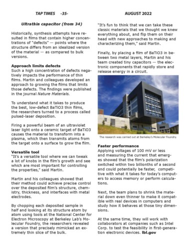
        plasma, which then transmits atoms from                  The research was carried out at Berkeley’s Molecular Foundry.
        the target onto a surface to grow the film.
                                                                Faster performance
        Versatile tool                                          Applying voltages of 100 mV or less
        “It’s a versatile tool where we can tweak               and measuring the current that emerg-
        a lot of knobs in the film’s growth and see             es showed that the film’s polarization
        which are most important for controlling                switched within two billionths of a second
        the properties,” said Martin.                           and could potentially be faster,   competi-
                                                                tive with what it takes for today’s comput-
        Martin and his colleagues showed that                   ers to access memory or perform calcula-
        their method could achieve precise control              tions.
        over the deposited film’s structure, chem-
        istry, thickness, and interfaces with metal             Next, the team plans to shrink the mate-
        electrodes.                                             rial down even thinner to make it compat-
                                                                ible with real devices in computers and
        By chopping each deposited sample in                    study how it behaves at those tiny dimen-
        half and looking at its structure atom by               sions.
        atom using tools at the National Center for
        Electron Microscopy at Berkeley Lab’s Mo-               At the same time, they will work with
        lecular Foundry, the researchers revealed               collaborators at companies such as Intel
        a version that precisely mimicked an ex-                Corp. to test the feasibility in first-genera-
        tremely thin slice of the bulk.                         tion electronic devices. lbl.gov

